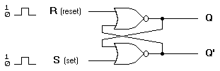
(a) Logic diagram
(b) Truth table
Figure 2. Basic flip-flop circuit with NOR gates
http://www.elec.uq.edu.au/~3e211/pracs/prac2/prac2.htm
Dept. of Computer Science and Electrical Engineering
The University of Queensland
St. Lucia  Qld  4072  Australia
The memory elements in a sequential circuit are called flip-flops. A flip-flop circuit has two outputs, one for the normal value and one for the complement value of the stored bit. Binary information can enter a flip-flop in a variety of ways and gives rise to different types of flip-flops.
A flip-flop circuit can be constructed from two NAND gates or two NOR gates. These flip-flops are shown in Figure 2 and Figure 3. Each flip-flop has two outputs, Q and Q', and two inputs, set and reset. This type of flip-flop is referred to as an SR flip-flop or SR latch. The flip-flop in Figure 2 has two useful states. When Q=1 and Q'=0, it is in the set state (or 1-state). When Q=0 and Q'=1, it is in the clear state (or 0-state). The outputs Q and Q' are complements of each other and are referred to as the normal and complement outputs, respectively. The binary state of the flip-flop is taken to be the value of the normal output.
When a 1 is applied to both the set and reset inputs of the flip-flop in Figure 2, both Q and Q' outputs go to 0. This condition violates the fact that both outputs are complements of each other. In normal operation this condition must be avoided by making sure that 1's are not applied to both inputs simultaneously.
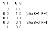
(a) Logic diagram
(b) Truth table
Figure 2. Basic flip-flop circuit with NOR gates
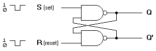
(a) Logic diagram
(b) Truth table
Figure 3. Basic flip-flop circuit with NAND gates
The NAND basic flip-flop circuit in Figure 3(a) operates with inputs normally at 1 unless the state of the flip-flop has to be changed. A 0 applied momentarily to the set input causes Q to go to 1 and Q' to go to 0, putting the flip-flop in the set state. When both inputs go to 0, both outputs go to 1. This condition should be avoided in normal operation.
The clocked SR flip-flop shown in Figure 4 consists of a basic NOR flip-flop and two AND gates. The outputs of the two AND gates remain at 0 as long as the clock pulse (or CP) is 0, regardless of the S and R input values. When the clock pulse goes to 1, information from the S and R inputs passes through to the basic flip-flop. With both S=1 and R=1, the occurrence of a clock pulse causes both outputs to momentarily go to 0. When the pulse is removed, the state of the flip-flop is indeterminate, ie., either state may result, depending on whether the set or reset input of the flip-flop remains a 1 longer than the transition to 0 at the end of the pulse.
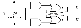
(a) Logic diagram
(b) Truth table
Figure 4. Clocked SR flip-flop
The D flip-flop shown in Figure 5 is a modification of the clocked SR flip-flop. The D input goes directly into the S input and the complement of the D input goes to the R input. The D input is sampled during the occurrence of a clock pulse. If it is 1, the flip-flop is switched to the set state (unless it was already set). If it is 0, the flip-flop switches to the clear state.
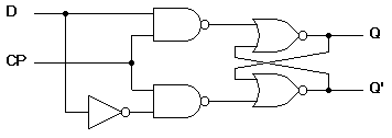
(a) Logic diagram with NAND gates
(b) Graphical symbol

(c) Transition table
Figure 5. Clocked D flip-flop
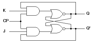
A JK flip-flop is a refinement of the SR flip-flop in that the indeterminate state of the SR type is defined in the JK type. Inputs J and K behave like inputs S and R to set and clear the flip-flop (note that in a JK flip-flop, the letter J is for set and the letter K is for clear). When logic 1 inputs are applied to both J and K simultaneously, the flip-flop switches to its complement state, ie., if Q=1, it switches to Q=0 and vice versa.
A clocked JK flip-flop is shown in Figure 6. Output Q is ANDed with K and CP inputs so that the flip-flop is cleared during a clock pulse only if Q was previously 1. Similarly, ouput Q' is ANDed with J and CP inputs so that the flip-flop is set with a clock pulse only if Q' was previously 1.
Note that because of the feedback connection in the JK flip-flop, a CP signal which remains a 1 (while J=K=1) after the outputs have been complemented once will cause repeated and continuous transitions of the outputs. To avoid this, the clock pulses must have a time duration less than the propagation delay through the flip-flop. The restriction on the pulse width can be eliminated with a master-slave or edge-triggered construction. The same reasoning also applies to the T flip-flop presented next.
(a) Logic diagram
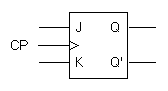
(b) Graphical symbol

(c) Transition table
Figure 6. Clocked JK flip-flop
The T flip-flop is a single input version of the JK flip-flop. As shown in Figure 7, the T flip-flop is obtained from the JK type if both inputs are tied together. The output of the T flip-flop "toggles" with each clock pulse.
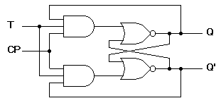
(a) Logic diagram
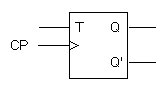
(b) Graphical symbol

(c) Transition table
Figure 7. Clocked T flip-flop
The state of a flip-flop is changed by a momentary change in the input signal. This change is called a trigger and the transition it causes is said to trigger the flip-flop. The basic circuits of Figure 2 and Figure 3 require an input trigger defined by a change in signal level. This level must be returned to its initial level before a second trigger is applied. Clocked flip-flops are triggered by pulses.
The feedback path between the combinational circuit and memory elements in Figure 1 can produce instability if the outputs of the memory elements (flip-flops) are changing while the outputs of the combinational circuit that go to the flip-flop inputs are being sampled by the clock pulse. A way to solve the feedback timing problem is to make the flip-flop sensitive to the pulse transition rather than the pulse duration.
The clock pulse goes through two signal transitions: from 0 to 1 and the return from 1 to 0. As shown in Figure 8 the positive transition is defined as the positive edge and the negative transition as the negative edge.
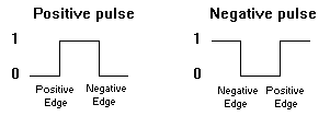
Figure 8. Definition of clock pulse transition
The clocked flip-flops already introduced are triggered during the positive edge of the pulse, and the state transition starts as soon as the pulse reaches the logic-1 level. If the other inputs change while the clock is still 1, a new output state may occur. If the flip-flop is made to respond to the positive (or negative) edge transition only, instead of the entire pulse duration, then the multiple-transition problem can be eliminated.
A master-slave flip-flop is constructed from two seperate flip-flops. One circuit serves as a master and the other as a slave. The logic diagram of an SR flip-flop is shown in Figure 9. The master flip-flop is enabled on the positive edge of the clock pulse CP and the slave flip-flop is disabled by the inverter. The information at the external R and S inputs is transmitted to the master flip-flop. When the pulse returns to 0, the master flip-flop is disabled and the slave flip-flop is enabled. The slave flip-flop then goes to the same state as the master flip-flop.
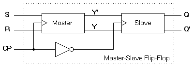
Figure 9. Logic diagram of a master-slave flip-flop
The timing relationship is shown in Figure 10 and is assumed that the flip-flop is in the clear state prior to the occurrence of the clock pulse. The output state of the master-slave flip-flop occurs on the negative transition of the clock pulse. Some master-slave flip-flops change output state on the positive transition of the clock pulse by having an additional inverter between the CP terminal and the input of the master.

Figure 10. Timing relationship in a master slave flip-flop
Another type of flip-flop that synchronizes the state changes during a clock pulse transition is the edge-triggered flip-flop. When the clock pulse input exceeds a specific threshold level, the inputs are locked out and the flip-flop is not affected by further changes in the inputs until the clock pulse returns to 0 and another pulse occurs. Some edge-triggered flip-flops cause a transition on the positive edge of the clock pulse (positive-edge-triggered), and others on the negative edge of the pulse (negative-edge-triggered). The logic diagram of a D-type positive-edge-triggered flip-flop is shown in Figure 11.
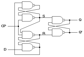
Figure 11. D-type positive-edge triggered flip-flop
When using different types of flip-flops in the same circuit, one must ensure that all flip-flop outputs make their transitions at the same time, ie., during either the negative edge or the positive edge of the clock pulse.
Flip-flops in IC packages sometimes provide special inputs for setting or clearing the flip-flop asynchronously. They are usually called preset and clear. They affect the flip-flop without the need for a clock pulse. These inputs are useful for bringing flip-flops to an intial state before their clocked operation. For example, after power is turned on in a digital system, the states of the flip-flops are indeterminate. Activating the clear input clears all the flip-flops to an initial state of 0. The graphic symbol of a JK flip-flop with an active-low clear is shown in Figure 12.
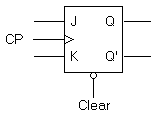
(a) Graphic Symbol
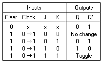
(b) Transition table
Figure 12. JK flip-flop with direct clear
Prepare the following in your prac book:
Basic Flip-Flop
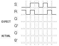
Figure 13. NOR gate flip-flop timing diagram
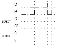
Figure 14. NAND gate flip-flop timing diagram
Master-Slave Flip-Flop
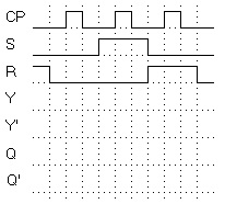
Figure 15. SR master-slave flip-flop timing diagram
Edge Triggered Flip-Flop
Figure 16. D-type edge triggered flip-flop timing diagram
Use LogicWorks to simulate the circuits that you have prepared. Use switches from the I/O library for the inputs and probes from the I/O library for the outputs. Place signal names on the circuit so that the signals are visible in the timing window. Create a separate drawing for each circuit.
To be sure that your circuits don't cross the printing page boundaries, check the Show Page Outlines option from the Drawing|Display Options... menu.
Only print out the circuit and waveforms for the SR master-slave flip-flop.